No funding issue for semicon projects, committed Rs 62K cr incentive: Meity | News

)
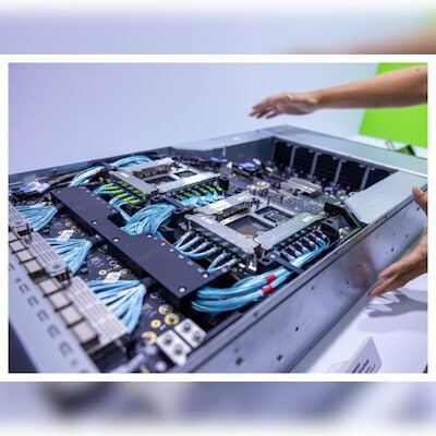
The government has received around 20 proposals for the Centre’s incentive under the India Semiconductor Mission. | Representational Photo
The government has committed about Rs 62,000 crore in incentives for electronic plants and there is no issue in funding semiconductor projects, Electronics and IT Secretary S Krishnan has said.
He told PTI that out of Rs 76,000 crore approved earlier, the government still has scope to accommodate small projects and will approach authorities when there are new projects in place.
“Out of the Rs 76,000 crore intended for the semiconductor mission, we have committed about Rs 62,000 crore, including the last scheme which was cleared for Kaynes. As of now, wherever claims have come up, we are settling them with maximum dispatch, and there is no funding issue right now at all,” Krishnan said.
The government has approved five semiconductor projects entailing investments of around Rs 1.52 lakh crore or about USD 18 billion.
He said that some funding is required for the Semiconductor Laboratory’s modernization in Mohali.
“We still have some funds to take up some smaller projects and approve them. Thereafter, we will have to go back to Ministry of Finance and Cabinet for approval when some new proposals come,” Krishnan said.
He said there is a high level of commitment from the government to make sure the semiconductor mission works.
“If additional funding is required, I am confident we will be able to secure it. As of now, wherever claims have come up, we are settling them with maximum dispatch, and there is no funding issue right now at all,” Krishnan said.
The government has received around 20 proposals for the Centre’s incentive under the India Semiconductor Mission.
Krishnan said India is targeting legacy nodes–the established technology segment in semiconductor space, which will produce large size chips.
The large size chips in the node of 28 nanometer, 40 nanometer, 60 and 65 nanometer can be used in big products like cars, electric vehicles, power inverters, consumer durables like washing machines, consumer electronic products etc.
“We are balancing the fact that it is reasonably well established technology and there is a considerable market for chips in that size for a range of industries. We have an established market here in the country for that. Therefore, we are focusing on those goals where the total cost of setting up a new facility is also not too great, which means that the subsidy outgo on behalf of India will be a little less and there is a significant demand as well,” Krishnan said.
He said India has a significant presence in the design ecosystem with 20 per cent of the global human resources required for semiconductor design based out of India.
Krishnan said many large brand names actually design in India.
“We never had a big presence in the manufacturing space. It is not a normal manufacturing process. There are a lot of precision , engineering skills, and purity involved. Therefore we do require, at least initially, some foreign collaboration and others who are leaders in this space to actually establish such facilities here in India. Once Indian companies, in collaboration with the overseas companies, are able to establish this, we expect the transfer of technology will take place in due course,” he said.
Krishnan said due to the prevailing geopolitical situation, like-minded countries are collaborating with India to make it a major semiconductor manufacturing destination.
(Only the headline and picture of this report may have been reworked by the Business Standard staff; the rest of the content is auto-generated from a syndicated feed.)
First Published: Sep 10 2024 | 2:49 PM IST


